The Seattle Daily Journal of Commerce (DJC) has selected 12 finalists including the Nanoengineering & Sciences Building for the 2017 Building of the Year award. Cast your vote for NanoES here!
Vote for NanoES as 2017 Building of the Year!
The Seattle Daily Journal of Commerce (DJC) has selected 12 finalists including the Nanoengineering & Sciences Building for the 2017 Building of the Year award. Cast your vote for NanoES here!

The 3rd annual NNCI conference will be held in Seattle at the University of Washington, September 13-14, 2018!
via UW News:
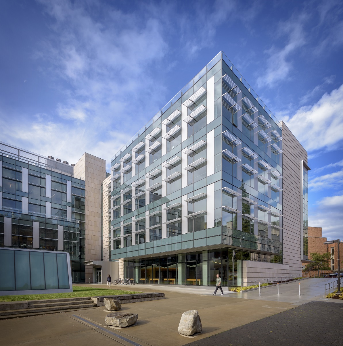
The University of Washington has launched a new institute aimed at accelerating research at the nanoscale: the Institute for Nano-Engineered Systems, or NanoES. Housed in a new, multimillion-dollar facility on the UW’s Seattle campus, the institute will pursue impactful advancements in a variety of disciplines — including energy, materials science, computation and medicine. Yet these advancements will be at a technological scale a thousand times smaller than the width of a human hair.
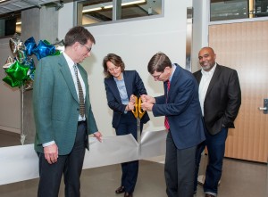
The institute was launched at a reception Dec. 4 at its headquarters in the $87.8-million Nano Engineering and Sciences Building. During the event, speakers including UW officials and NanoES partners celebrated the NanoES mission to capitalize on the university’s strong record of research at the nanoscale and engage partners in industry at the onset of new projects.
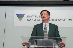
The vision of NanoES, which is part of the UW’s College of Engineering, is to act as a magnet for researchers in nanoscale science and engineering, with a focus on enabling industry partnership and entrepreneurship at the earliest stages of research projects. According to Karl Böhringer, director of the NanoES and a UW professor of electrical engineering and bioengineering, this unique approach will hasten the development of solutions to the field’s most pressing challenges: the manufacturing of scalable, high-yield nano-engineered systems for applications in information processing, energy, health and interconnected life.
“The University of Washington is well known for its expertise in nanoscale materials, processing, physics and biology — as well as its cutting-edge nanofabrication, characterization and testing facilities,” said Böhringer, who stepped down as director of the UW-based Washington Nanofabrication Facility to lead the NanoES. “NanoES will build on these strengths, bringing together people, tools and opportunities to develop nanoscale devices and systems.”
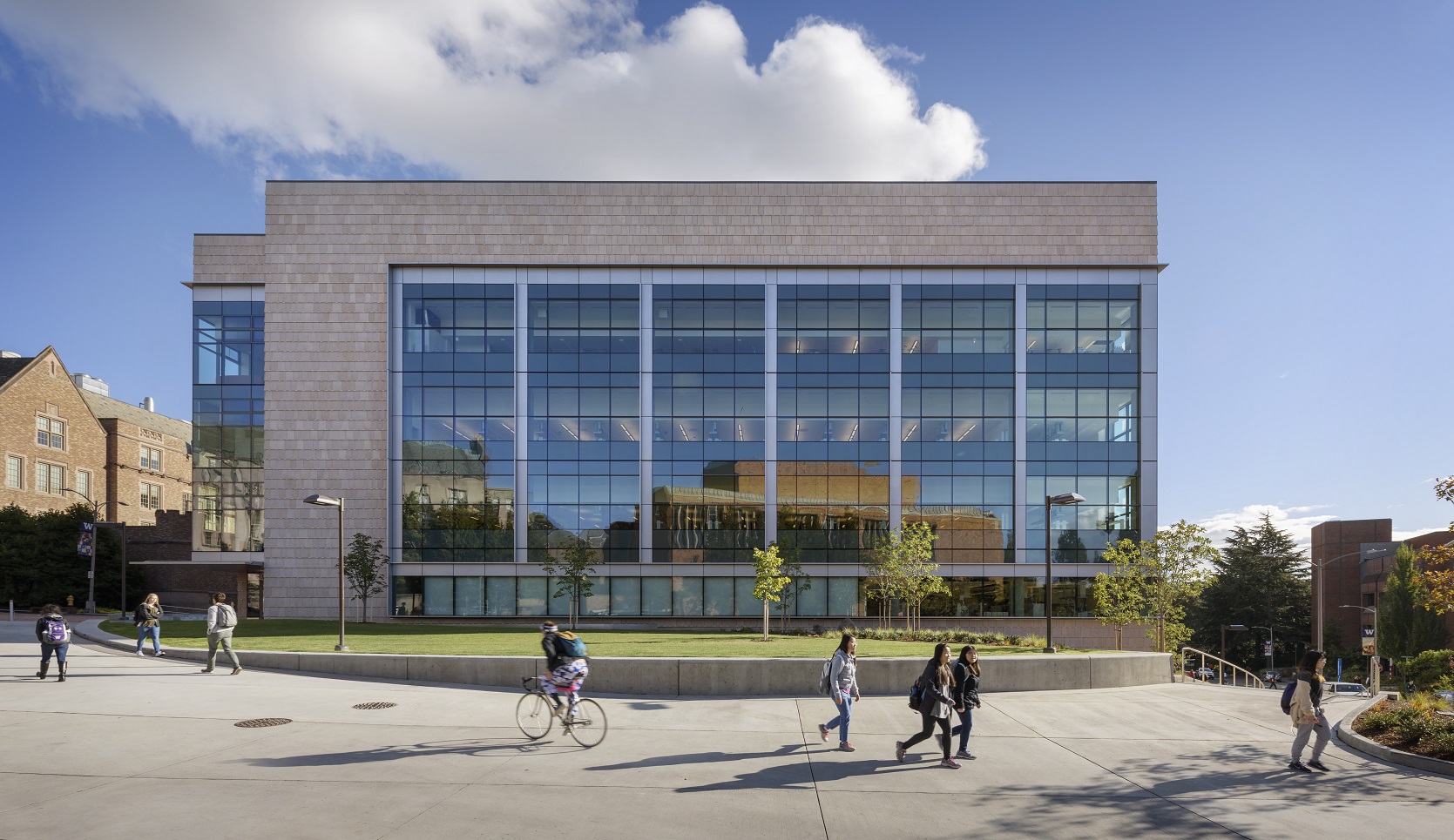
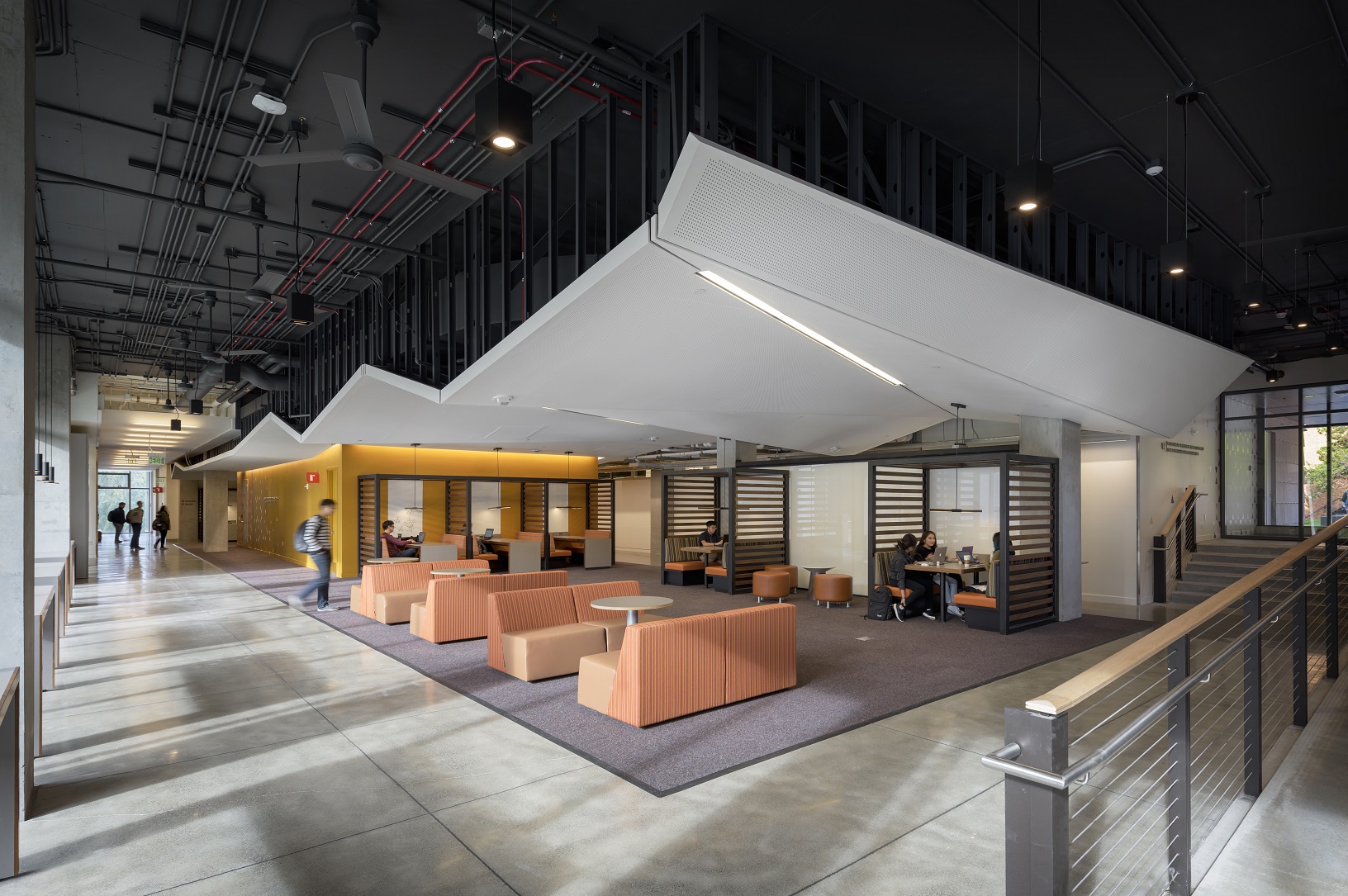
The centerpiece of the NanoES is its headquarters, the Nano Engineering and Sciences Building. The building houses 90,300 square feet of research and learning space, and was funded largely by the College of Engineering and Sound Transit. It contains an active learning classroom, a teaching laboratory and a 3,000-square-foot common area designed expressly to promote the sharing and exchanging of ideas. The remainder includes “incubator-style” office space and more than 40,000 square feet of flexible multipurpose laboratory and instrumentation space. The building’s location and design elements are intended to limit vibrations and electromagnetic interference so it can house sensitive experiments.
NanoES will house research in nanotechnology fields that hold promise for high impact, such as:
Collaborations with other UW-based institutions will provide additional resources for the NanoES. Endeavors in scalable nanomanufacturing, for example, will rely on the roll-to-roll processing facility at the UW Clean Energy Institute‘s Washington Clean Energy Testbeds or on advanced surface characterization capabilities at the Molecular Analysis Facility. In addition, the Washington Nanofabrication Facility recently completed a three-year, $37 million upgrade to raise it to an ISO Class 5 nanofabrication facility.
UW faculty and outside collaborators will build new research programs in the Nano Engineering and Sciences Building. Eric Klavins, a UW professor of electrical engineering, recently moved part of his synthetic biology research team to the building, adjacent to his collaborators in the Molecular Engineering & Sciences Institute and the Institute for Protein Design.
“We are extremely excited about the interdisciplinary and collaborative potential of the new space,” said Klavins.
The NanoES also has already produced its first spin-out company, Tunoptix, which was co-founded by Böhringer and recently received startup funding from IP Group, a U.K.-based venture capital firm.
“IP Group is very excited to work with the University of Washington,” said Nena Golubovic, physical sciences director for IP Group. “We are looking forward to the new collaborations and developments in science and technology that will grow from this new partnership.”
“We are eager to work with our partners at the IP Group to bring our technology to the market, and we appreciate their vision and investment in the NanoES Integrated Photonics Initiative,” said Tunoptix entrepreneurial lead Mike Robinson. “NanoES was the ideal environment in which to start our company.”
The NanoES leaders hope to forge similar partnerships with researchers, investors and industry leaders to develop technologies for portable, wearable, implantable and networked nanotechnologies for personalized medical care, a more efficient interconnected life and interconnected mobility. In addition to expertise, personnel and state-of-the-art research space and equipment, the NanoES will provide training, research support and key connections to capital and corporate partners.
“We believe this unique approach is the best way to drive innovations from idea to fabrication to scale-up and testing,” said Böhringer. “Some of the most promising solutions to these huge challenges are rooted in nanotechnology.”
The NanoES is supported by funds from the College of Engineering and the National Science Foundation, as well as capital investments from investors and industry partners.
Title: Silicon Integrated Circuit, Sensor, and System Approaches for Lab-on-CMOS Applications
Date & Time: Tuesday, Nov. 28th, 10:30-11:30 am
Location: 105 EEB
Abstract: The Lab-on-CMOS research community leverages the power and economies of scale of modern silicon integrated circuits, built up over the previous fifty years for high-performance computation and imaging, for low-cost chemical and biological sensing applications. The integration of new materials, sensing modalities, and intelligent computation in CMOS-based sensor platforms enables a broad range of miniaturized diagnostic, therapeutic, and continuous monitoring systems. In this talk, I will present a survey of ongoing research in my lab focused on the chip-level development and system-level integration of IC-based sensors for physical, chemical, and biological sensing. This includes CMOS-integrated single-photon detectors, high dynamic range visible light sensing, on-chip high-voltage sensor biasing, low-voltage energy harvesting, and applications in radiation sensing and continuous biological monitoring. I will also describe our recently developed approach for the planar integration of IC-based sensors with microfluidic sample delivery using scalable, manufacturable processes.
Bio (IEEE): Matthew L. Johnston received the B.S. degree in electrical engineering from the California Institute of Technology, Pasadena, CA, in 2005, and the M.S. and Ph.D. degrees in electrical engineering from Columbia University, New York, NY, in 2006 and 2012, respectively.
He is currently an Assistant Professor in the School of Electrical Engineering and Computer Science at Oregon State University. He was co-founder and manager of research at Helixis, a Caltech-based spinout developing instrumentation for real-time PCR, from 2007 until its acquisition by Illumina in 2010. From 2012 to 2013 he was a postdoctoral scholar in the Bioelectronic Systems Lab at Columbia University. He is a co-founder of Chimera Instruments, which designs high-speed electrophysiology amplifiers for biophysics research, and previously founder of Bialanx, which was awarded an NSF SBIR Grant in 2013 for work in radiation biodosimetry.
Prof. Johnston currently runs the Sensors and Integrated Microelectronics Laboratory (SIM Lab) at Oregon State University, which leverages custom CMOS IC design and post-fabrication to build miniaturized sensor systems. His current research interests include integration of sensors and transducers with active CMOS substrates, lab-on-CMOS platforms for label-free chemical and biological sensing, and low-power distributed sensing applications.
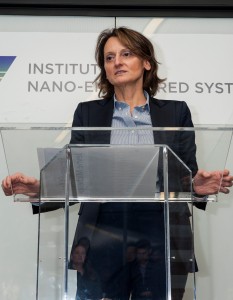
Please join us for the inaugural lecture by Distinguished Practitioners in Nano-engineered Systems. This new seminar series is organized by the Institute for Nano-engineered Systems and focuses on individuals who are making outstanding contributions to the development of microsystems and nanotechnology with significant commercial and societal impact.

Nena Golubovic, Ph.D.
Director, Physical Sciences
IP Group, Inc.
Tuesday, December 5, 12:30 – 1:20 pm
Anderson 223
Our inaugural Distinguished Practitioner in Nano-engineered Systems will venture back in time and briefly cover the evolution of micro and nano electro mechanical systems (MEMS/NEMS), then focus the bulk of the presentation on early stage investing before finishing up with an outlook on collaborations between IP Group and UW.
Nena joined IP Group in 2014, and currently oversees the Physical Sciences sector in North America. As part of the senior management team she works on a variety of early stage investments transitioning from IP Group’s partner network research labs to the marketplace.
Nena has extensive experience developing and commercializing cutting edge micro-technology products for automotive, consumer and medtech industries. She spent her 20-year career in medium public, private and small start-up environments. Nena served as Vice President of Medical Products at Apogee Technologies where she led commercialization of micro-structured transdermal systems for drug delivery. Prior to that she was Director of New Product Development at Standard MEMS where she led commercialization and manufacturing scaleup of the world’s first MEMS microphone. She collaborated with Xerox, Lexmark, Kavlico, Becton Dickinson and the likes in developing uniquely differentiated, micro-technology enabled, new product generations for applications across different market segments. Nena was involved in various product development, go-to-market and management roles with several early stage start-up companies commercializing university technologies.
Nena holds a Ph.D. and M.S. in Electrical Engineering from the University of Cincinnati, and a B.S. in Engineering Physics from the University of Belgrade.
The University of Louisville, a partner in the NSF National Nanotechnology Coordinated Infrastructure (NNCI) network, is recruiting students in the interdisciplinary field of advanced micro/nano manufacturing engineering through exciting hands-on research projects with applications in healthcare, energy, advanced manufacturing, security and the environment. Read the flyer for more information.
The Society of Physics Students is hosting a Science Café on quantum information on Friday, November 17, 3:30 – 5:00 pm at Café Allegro, 4214 University Way NE. It will be an event targeting the general public as an audience.
 You’re Invited!
Participate in the kick-off of the Institute for Nano-engineered Systems as we celebrate the opening of the Nano Engineering & Sciences Building.
We cordially invite you to the NanoES Building Ribbon Cutting Ceremony.
Join us afterwards for an evening of networking with food and drinks.
The École Polytechnique Fédérale de Lausanne (EPFL) will soon offer a self-paced MOOC class on micro and nano fabrication for MEMS.
Supercapacitors are an aptly named type of device that can store and deliver energy faster than conventional batteries. They are in high demand for applications including electric cars, wireless telecommunications and high-powered lasers.