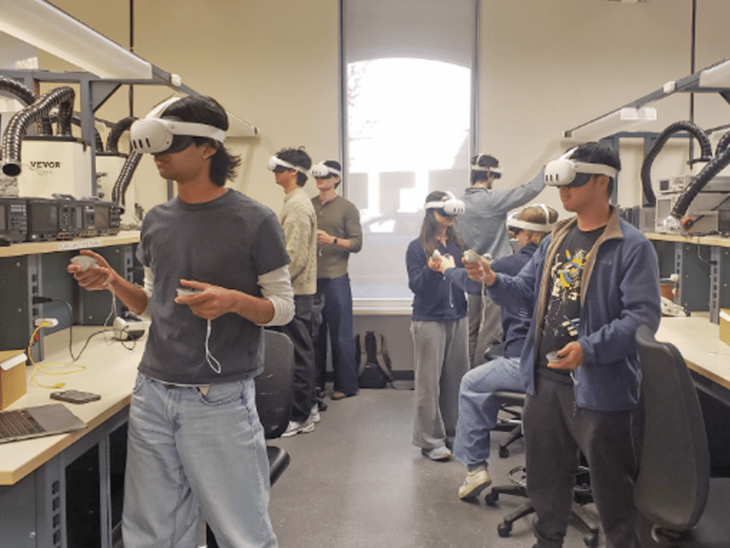
Skip to content

News & Events

2023 Plenty of Beauty at the Bottom

Every year in honor of National Nanotechnology Day on October 9th, the National Nanotechnology Coordinated Infrastructure (NNCI) hosts a Plenty of Beauty at the Bottom image contest to celebrate the beauty of the micro and nanoscale. Check out this year’s winners and featured images.

A new kind of chip for quantum technology

Today, we are living in the midst of a race to develop a quantum computer, one that could be used for practical applications. This device, built on the principles of quantum mechanics, holds the potential to perform computing tasks far beyond the capabilities of today’s fastest supercomputers. Quantum computers and other quantum-enabled technologies could foster significant advances in areas such as cybersecurity and molecular simulation, impacting and even revolutionizing fields such as online security, drug discovery and material fabrication.

NanoES announces 2023 Northwest Nanotechnology Seed Grant awardees

The UW Institute for Nano-engineered Systems (NanoES) has awarded three seed grants to UW researchers to use nanotechnology tools to develop new, innovative technologies and devices. Electrical & computer engineering (ECE) Postdoctoral Scholar Brant Bowers, ECE Assistant Professor Serena Eley and mechanical engineering Assistant Professor Mohammed Malakooti will receive up to $10,000 to carry out work in the UW’s Washington Nanofabrication Facility (WNF) and Molecular Analysis Facility (MAF). WNF and MAF are key nanotechnology facilities in the Northwest Nanotechnology Infrastructure, which is one of 16 sites in the NSF’s National Nanotechnology Coordinated Infrastructure (NNCI) program.

“We’ve had another excellent round of proposals for the Nanotechnology Seed Grants and the WNF and MAF teams are eager to support these researchers as they develop new technologies,” said NanoES Director and Professor of electrical & computer engineering and bioengineering at the UW, Karl Böhringer. “We’re excited to see where Brant’s work in reducing electric field noise, Serena’s in superconducting quantum circuits, and Mohammed’s in tactile sensors in robotics and wearable electronics leads.”

Nanotechnology Seed Grants enable first-time facility users both inside and outside the UW to build and characterize prototypes, obtain preliminary results and conduct proof of concept studies. Applications for 2024-25 support will open early in 2024. More information can be found here.

Correlation of Fabrication and Cleaning Processes with Materials Properties in Nano-fabricated Ion Traps,” by Bowers.

Abstract: Trapped ion quantum computers are plagued by electric field noise that is several orders of magnitude more than theory predicts. We seek to examine the materials characteristics, including but not limited to roughness, surface chemistry and crystallinity, of a variety of ion traps created through different fabrication and cleaning processes in order to identify the sources of this noise. These materials’ characteristics will compare to measurements of this electric field noise in ion-trap operation through motional heating measurements. Previous studies of the correlation between fabrication/cleaning procedures, the resulting materials properties and the electric field noise in those traps have been limited to one or two traps and one or two diagnostics. We seek to implement a more thorough study of materials properties using the systems at the MAF. With no prior information about what properties are important for surface noise, we plan to begin with a scattershot approach: measuring with the atomic force microscopes, ellipsometer, profilometer, secondary ion mass spectrometer, Raman microscope, scanning electron microscope, x-ray diffraction spectrometers and x-ray photoelectron spectrometer.  We will compare a set of three fabrication techniques, electroplating, sputtering, electron-beam evaporation, and three cleaning techniques, argon-ion milling, potassium hydroxide potential sweep and piranha acid. This leads to nine total traps to analyze and compare. This fund will enable us to train a new user in the use of these tools and enable the preliminary stages of the first systematic study of the impacts of cleaning and fabrication methodology on surface noise in ion traps. These results can then be used to reduce electric field noise in ion traps, improving the scalability of trapped ion quantum computers.


Serena Eley

Superconducting Quantum Circuits Based on Epitaxial Nitrides,” by Elay.

Abstract: The performance of superconducting quantum circuits is limited by energy losses from parasitic two-level fluctuators (TLFs). Although the precise microscopic origins of this decoherence mechanism are not completely understood, it can be traced to defects in the superconductor, at interfaces, and in the tunneling barrier in Josephson junctions (JJs). This may be remedied by the use of structurally and chemically matched epitaxial materials stacks, which may ultimately produce qubits having greater coherence times. However, few studies have successfully fabricated fully epitaxial JJs and the coherence times remain below that of commonly used aluminum/aluminum oxide/aluminum JJs. These are known to host a high density of parasitic TLFs. Consequently, the superiority of epitaxy remains unproven, however, few fully epitaxial material systems have been explored.

To address this issue, in collaboration with Rigetti Computing, the National Renewable Energy Lab (NREL), and Lawrence Berkeley National Lab (LBNL), we will study a new material family for superconducting qubits. We will test a platform of transition metal nitride superconductors and ternary nitride barrier layers to fabricate JJs and transmon qubits prepared with clean stacks of crystallographically matched interfaces, starting with niobium nitride (NbN) as the superconductor and magnesium niobium nitride (Mg2NbN3) as the barrier. We hypothesize that this will lead to reduced deleterious defect populations relative to current materials, enabling long coherence times. Our initial tasks are to: grow fully epitaxial stacks of NbN/Mg2NbN3/NbN in a new ultra-high-vacuum sputtering tool at the LBNL Molecular Foundry (MF), characterize structural and superconducting properties of the stack, nanofabricate epitaxial JJs at the Washington Nanofabrication Facility (WNF), measure low-temperature transport properties of JJs in the Eley Lab at UW to determine critical parameters and fabricate/measure qubits inside a 3D cavity in a dilution cryostat at Rigetti Computing.


Mohammad Malakooti

A Soft, Multimodal Tactile Sensor for Robotics and Wearable Electronics,” by Malakooti.

Abstract: Tactile sensors have emerged as a revolutionary technology capable of detecting and measuring physical contact, pressure and force. These sensors have found applications in soft robotics, wearable electronics and human-computer interactions. In the pursuit of developing advanced tactile sensing capabilities, our project proposes the creation of a soft, multimodal tactile sensor. One key aspect that sets our project apart is the utilization of room-temperature liquid metal (LM) alloys, particularly eutectic gallium indium. These alloys possess remarkable properties, including high conductivity and flowability due to their low viscosity. By employing LM within microchannels, we can effectively monitor changes in resistance within the deformed microfluidic device. This allows precise measurement of applied normal and shear forces.

The innovative nature of our project lies in the optimization of sensor sensitivity and robustness. We will focus on refining the geometry of the microchannels and enhancing the connection between the liquid conductors and solid wires. These improvements will result in a tactile sensor that exhibits exceptional sensitivity to a wide range of tactile stimuli while maintaining durability in various operating conditions. To optimize sensor sensitivity and robustness, we will employ a range of cutting-edge research techniques. We will fabricate new master molds for the designed microfluid devices in the WNF and MAF facility, utilizing specialized equipment to precisely control microchannel geometry. We will also conduct experiments to study the wettability of the microchannels and the role of the oxide interface as we fill them with LM. Through advanced simulations and modeling, we will analyze the performance of the sensor under different operating conditions and identify the optimal configuration for maximum sensitivity and durability. Finally, we will test the sensor’s performance under controlled conditions and accurately measure the applied force to demonstrate its effectiveness and potential impact on the field.


How UW ECE is ready for the CHIPS and Science Act

Semiconductors, also known as integrated circuits or microchips, have become a necessity for modern life. Long considered to be the brains of modern electronics, these tiny chips can be found in almost every electronic device in use today. And their impact is vast, supporting every sector of the U.S. economy, as well as national security. Currently, all major U.S. defense systems and platforms rely on microchips for their performance, and in many cases, simply to operate.

Researchers put a new twist on graphite

In a new Nature paper, a team led by UW researchers reports that it is possible to imbue graphite — the bulk, 3D material found in No. 2 pencils — with physical properties similar to graphite’s 2D counterpart, graphene. Not only was this breakthrough unexpected, the team also believes its approach could be used to test whether similar types of bulk materials can also take on 2D-like properties. If so, 2D sheets won’t be the only source for scientists to fuel technological revolutions. Bulk, 3D materials could be just as useful.

Reimagining optics for smartphones and other devices

UW ECE and Physics Associate Professor Arka Majumdar and UW ECE postdoctoral scholar Johannes Fröch are part of an international research team helping to make high-quality, color cameras smaller and lighter for mobile platforms, such as next-generation smartphones, drones, and point-of-care medical devices. The team recently developed a miniature camera that uses an innovative hybrid optical system over 100 times smaller than its commercial counterpart.