Mechanical Engineering (ME) researchers co-led by Mohammad Malakooti — NanoES faculty member and ME assistant professor — are applying an inverse design framework to identify new composite materials for flexible electronic and wearables. With funding from the National Science Foundation and the AI Institute in Dynamic Systems, the team is focusing on optimal material composition while reducing the number of experiments. Discover how machine learning and physics-based modeling are influencing the team’s innovative research.
A University of Washington course is using virtual reality modules to trainstudents for in-demand semiconductor jobs.Electrical & Computer Engineering Associate Professor Tai-Chang Chen adopted the Cornell NanoScale Facility (CNF) Virtual Reality (VR) educational platform for his Devices and Circuits 1 (EE 331) course this spring to offer students the job skills needed to fill the growing semiconductor technical workforce gap.
Semiconductor chips control electricity in just about every piece of modern technology. And since they are even smaller than microscopic airborne particles that can cause device failures, their production requires a controlled environment that only a cleanroom can provide.
Based on projections from the Semiconductor Industry Association, 67,000 semiconductor jobs in the United States will be unfilled by 2030 — that’s 58% of roles spanning across manufacturing and design. The CNF VR educational models make it possible to scale cleanroom training and support workforce development goals by reaching significantly more learners.
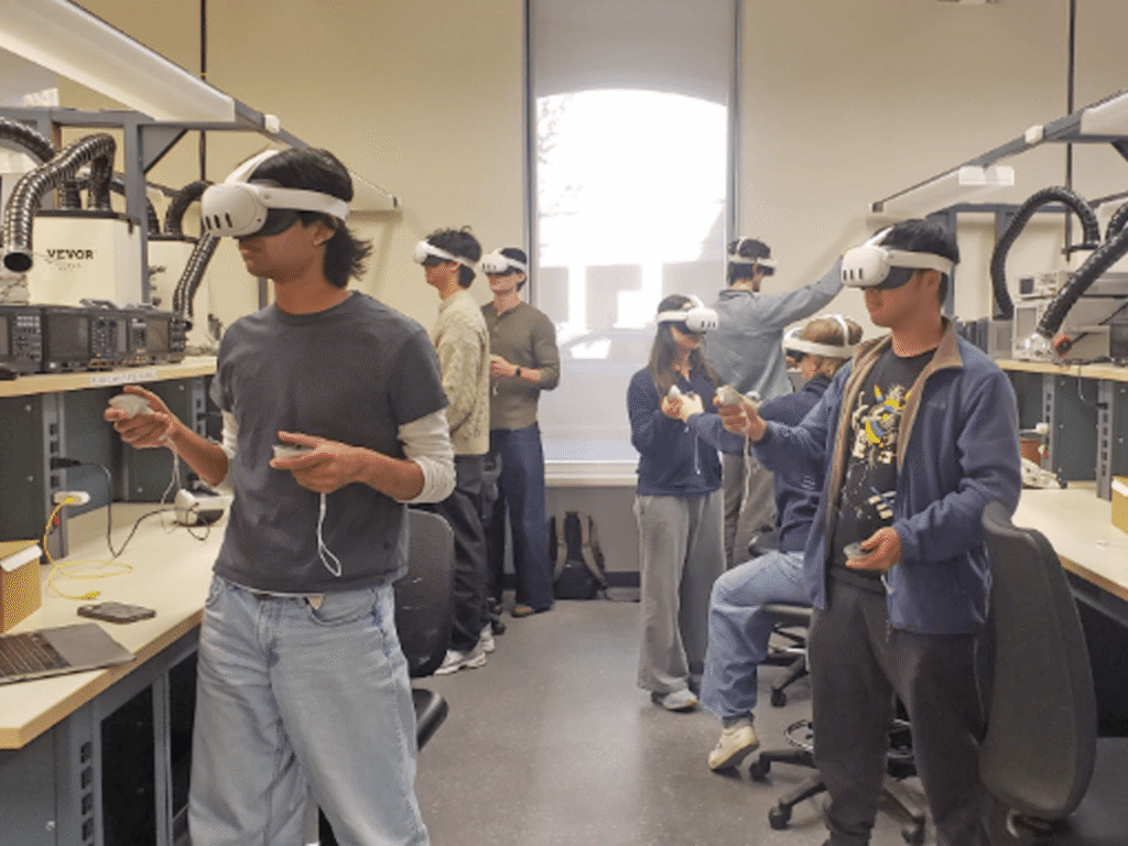
Students in EE331 are immersed in the cleanroom-user experience, which includes simulated face-to-face interactions with CNF equipment and staff. The course was equipped with eight Meta Quest 3 headsets (one per student, per lab section), along with licensed access to CNF’s library of immersive cleanroom modules, including:
Students engage with the content collaboratively in the EE 331 lab space, exploring cleanroom environments and processing tools that would otherwise be inaccessible at this scale. (Photo: UW UPWARDS)
“Incorporating CNF VR educational modules in the classroom offers UW students a unique edge in developing in-demand skills in the microelectronic and nanotechnology fields,” said Chen. “This opportunity highlights UW’s commitment to innovation, along with its role in strengthening the semiconductor industry as an UPWARDS for the Future Network partner.”
UW’s on-campus cleanroom is housed within the Washington Nanofabrication Facility (WNF) in Fluke Hall. WNF Acting Director Darick Baker worked with CNF and UPWARDS to enroll UW in the beta-test deployment and prepared the headsets for students.
With a potential shortage in a skilled cleanroom workforce in the next five to ten years, “many additional cleanroom workers are needed, but very few students are familiar with what semiconductor manufacturing requires,” noted Baker. “The CNF VR educational modules allow WNF and UW to introduce more students to the cleanroom environment,” noted Baker.
Students complete the modules in VR prior to their hands-on lab sessions, allowing them to enter the WNF better prepared and able to make more productive use of limited lab time. Early observations suggest that the VR platform meaningfully extends the reach of experiential learning in the EE331 course.
“Immersive VR content empowers students,” said Chen. “These innovative modules enhance the lab experience and provide students with both exposure and confidence to master cleanroom protocols — and ultimately contribute to filling the needs that come with the rapid growth of the semiconductor field.”
Additionally, Chen is exploring further integration through a planned UW–Japan study-abroad fabrication course developed in partnership with member institutions of the UPWARDS for the Future Network. In 2023, Micron and Tokyo Electron Limited (TEL) launched the UPWARDS for the Future Network alongside university partners. This partnership cultivates a more diverse, robust and highly skilled talent pipeline for the semiconductor workforce — and drives emerging research while increasing the pipeline of students studying a semiconductor curr
PINES (Pacific-Intermountain Network for Education in Semiconductors) has officially been selected as one of the Regional Nodes, which includes the Washington Nanofabrication Facility (WNF) at the University of Washington among its members. Led by Boise State University, the NNME Pacific Intermountain node serves Idaho, Washington, Oregon, Montana, Utah, Colorado, Nevada, Northern California and Hawaii.
“The launch of these Regional Nodes constitutes the activation of national infrastructure built to meet the most consequential economic and technological challenge of our time,” said Shari Liss, Vice President of Workforce Development and Initiatives at SEMI and the SEMI Foundation.
A research team led by Arka Majumdar, NanoES faculty member and UW Electrical & Computer Engineering (ECE) and Physics professor, has engineered a new type of optical microchip. This programmable photonic integrated circuit was fabricated in the Washington Nanofabrication Facility (WNF) and is low power, electrically reconfigurable, and can be mass-produced. Read more about this chip that has the potential to be applied in a wide range of technologies, including information processing, sensing, imaging, machine learning and artificial intelligence here.
NTEC provides experiential entrepreneurship education for teams led by undergraduates, graduate students and post-doctoral scholars. NTEC teams learn about the importance of customer discovery and how to leverage NNCI resources to develop a nanotechnology-enabled minimum viable product (MVP). The seven-week, virtual “at-your-pace” program culminates in a “pitch” event where teams share their progress with business leaders.
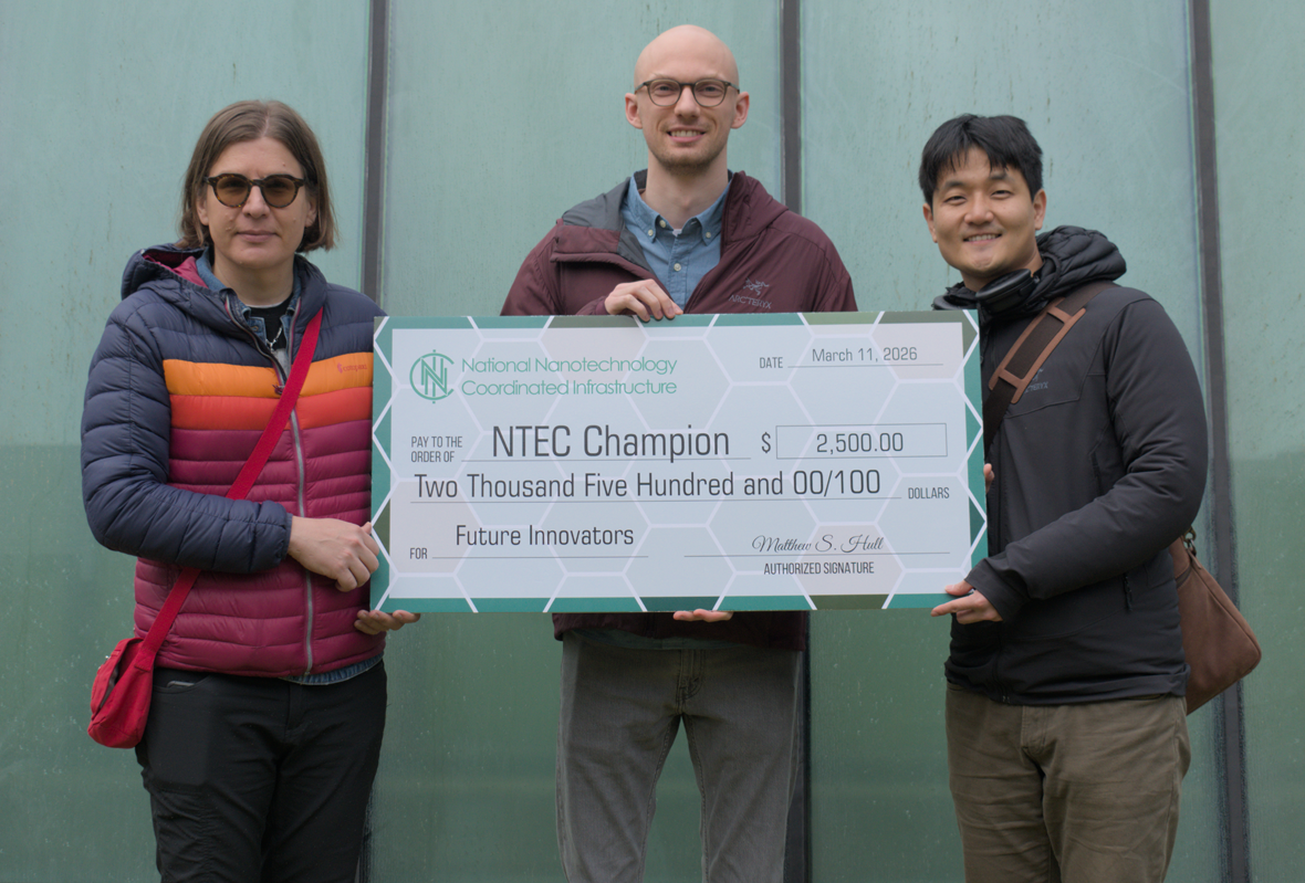
Led by CoMotion Postdoctoral Entrepreneurship Fellow Kevin Lee and PhD student Zach Wylie, the winning project from the Pozzo Research Group involves the development of next generation high-power-density battery electrodes for power-hungry applications that traditionally relied on diesel. The group will use the $2,500 award from NNCI to continue development and validation of their technology based on the group’s proprietary nanoparticles.
“Through customer-discovery work conducted with NNCI’s NTEC program, we’ve gained a clear understanding of the pain points faced by legacy battery manufacturers,” said Lee and Wylie.
Looking ahead, Lee and Wylie “plan on using NNCI’s facilities such as the Molecular Analysis Facility (MAF) and Washington Nanofabrication Facility (WNF) to characterize our material under industry-relevant conditions and generate data that manufacturers require to evaluate and ultimately adopt our material.”
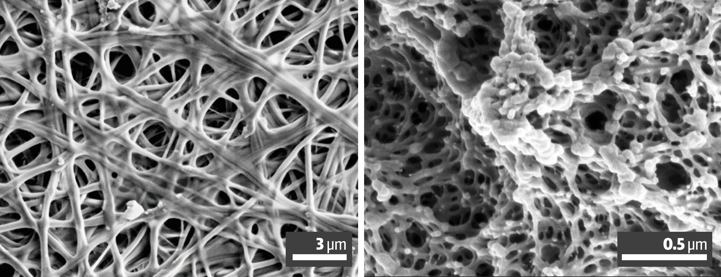
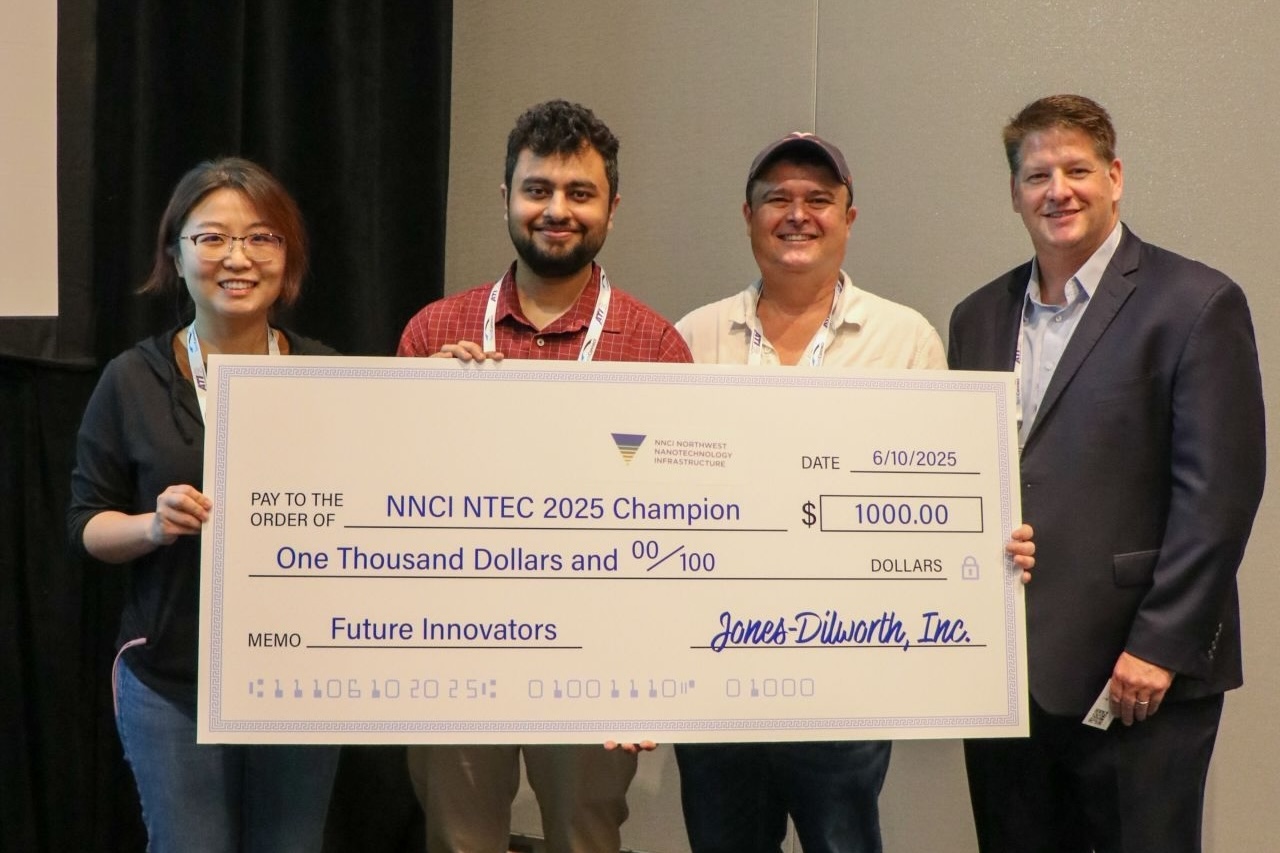
On June 10, 2025, Anmol Purohit, Dr. Ji Feng, and Almond Lau won first prize at the NNCI NTEC Showcase for their project, “Synthesis of metal-organic framework particles for removal of short and ultra-short chain PFAS from water”.
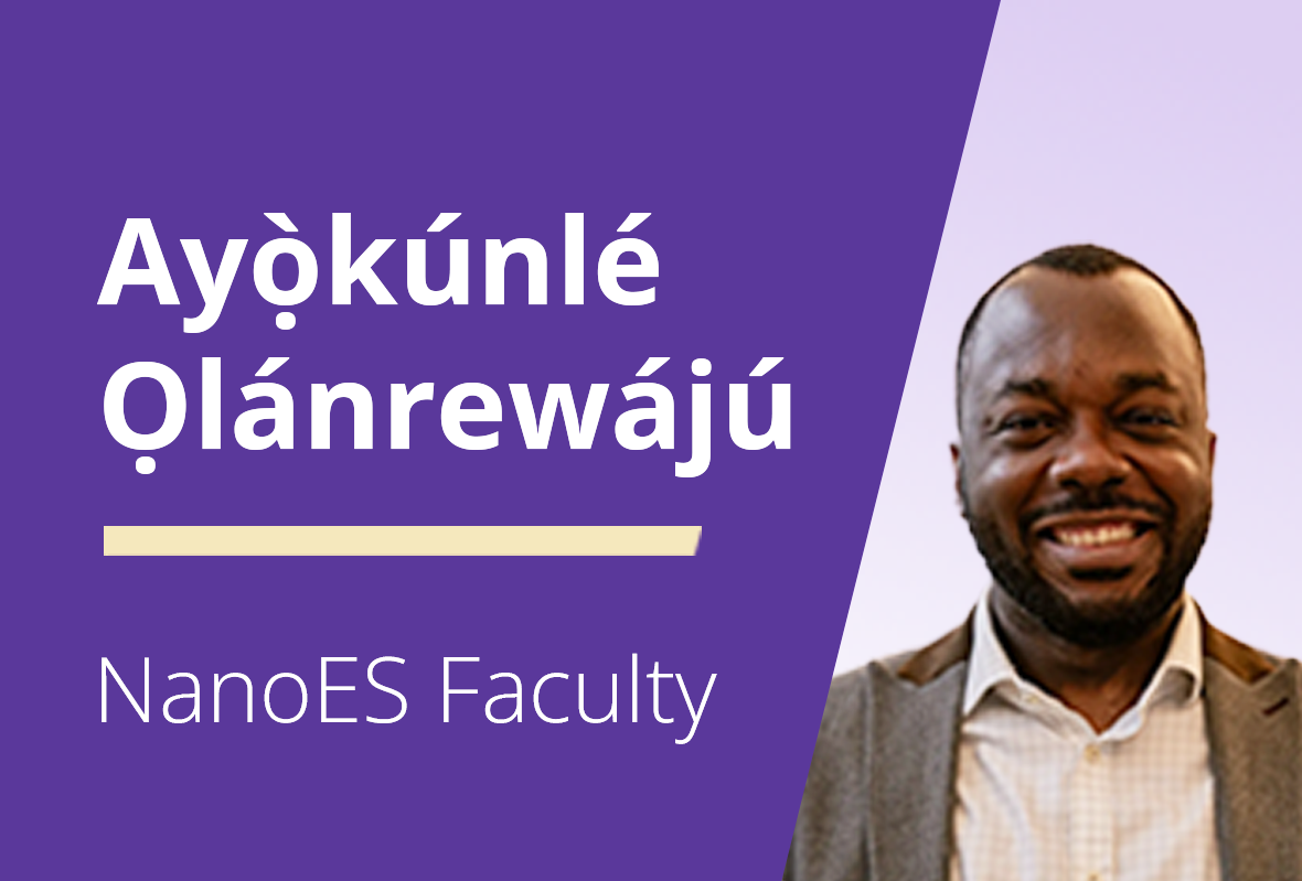
NanoES faculty member Ayokunle Olanrewaju (bioengineering, mechanical engineering) and collaborators Ashleigh Theberge and Erwin Berthier will develop a platform for at-home self-collection of blood, serum separation, and sample stabilization at sufficient sample volumes for comprehensive HIV monitoring.
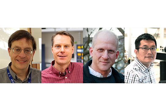
David Cobden (physics), David Ginger (chemistry), Charles Marcus (materials science & engineering, physics), and Xiaodong Xu (physics, materials science & engineering) have been recognized for significant influence in their chosen field or fields of research through the publication of multiple papers in the top 1% of citations over the last decade.