Skip to content

Light-based ‘tractor beam’ assembles materials at the nanoscale

A team led by NanoES faculty member Peter Pauzauskie, a professor of materials science and engineering, has developed a method that could make reproducible manufacturing at the nanoscale possible. The team adapted a light-based technology employed widely in biology — known as optical traps or optical tweezers — to operate in a water-free liquid environment of carbon-rich organic solvents, thereby enabling new potential applications.

Scientists can now control thermal profiles at the nanoscale

In a paper published online July 30 by the journal ACS Nano, David Masiello, NanoES faculty member and professor of chemistry, and colleagues from Rice University and Temple University, report a new breakthrough on controlling the thermal profiles of materials at the nanoscale. The team of researchers designed and tested an experimental system that uses a near-infrared laser to actively heat two gold nanorod antennae — metal rods designed and built at the nanoscale — to different temperatures. The nanorods are so close together that they are both electromagnetically and thermally coupled. Yet the team measured temperature differences between the rods as high as 20 degrees Celsius. By simply changing the wavelength of the laser, they could also change which nanorod was cooler and which was warmer, even though the rods were made of the same material.

First-ever visualizations of electrical gating effects on electronic structure could lead to longer-lasting devices

UW physicists David Cobden and Xiaodong Xu, in collaboration with colleagues at the University of Warwick, developed a technique to measure the energy and momentum of electrons in operating microelectronic devices made of atomically thin — so-called 2D — materials. Their findings, published last week in the journal Nature could lead to new, finely tuned, high-performance electronic devices.

Researchers take a bottom-up approach to synthesizing microscopic diamonds for bioimaging, quantum computing

NanoES faculty member Peter Pauzauskie and his team discovered that they can use extremely high pressure and temperature to introduce other elements into nanodiamonds, making them potentially useful in cell and tissue imaging, as well as quantum communications and quantum sensing. This work was done in collaboration with the U.S. Naval Research Laboratory and the Pacific Northwest National Laboratory and published in Science Advances on May 3.

Design, synthesis, and integration of quantum nanoscale materials

Peter Pauzauskie, Materials Science & Engineering professor and NanoES faculty member, synthesizes nanoscale materials for potential applications in next-generation quantum sensors, biomedical devices, and solid-state laser refrigeration. The Pauzauskie Research Group maintains office space, a wet lab for nanocrystal synthesis, and a lab for laser spectroscopy experiments in the NanoES building.

Request for Proposals – NanoES Research Initiatives

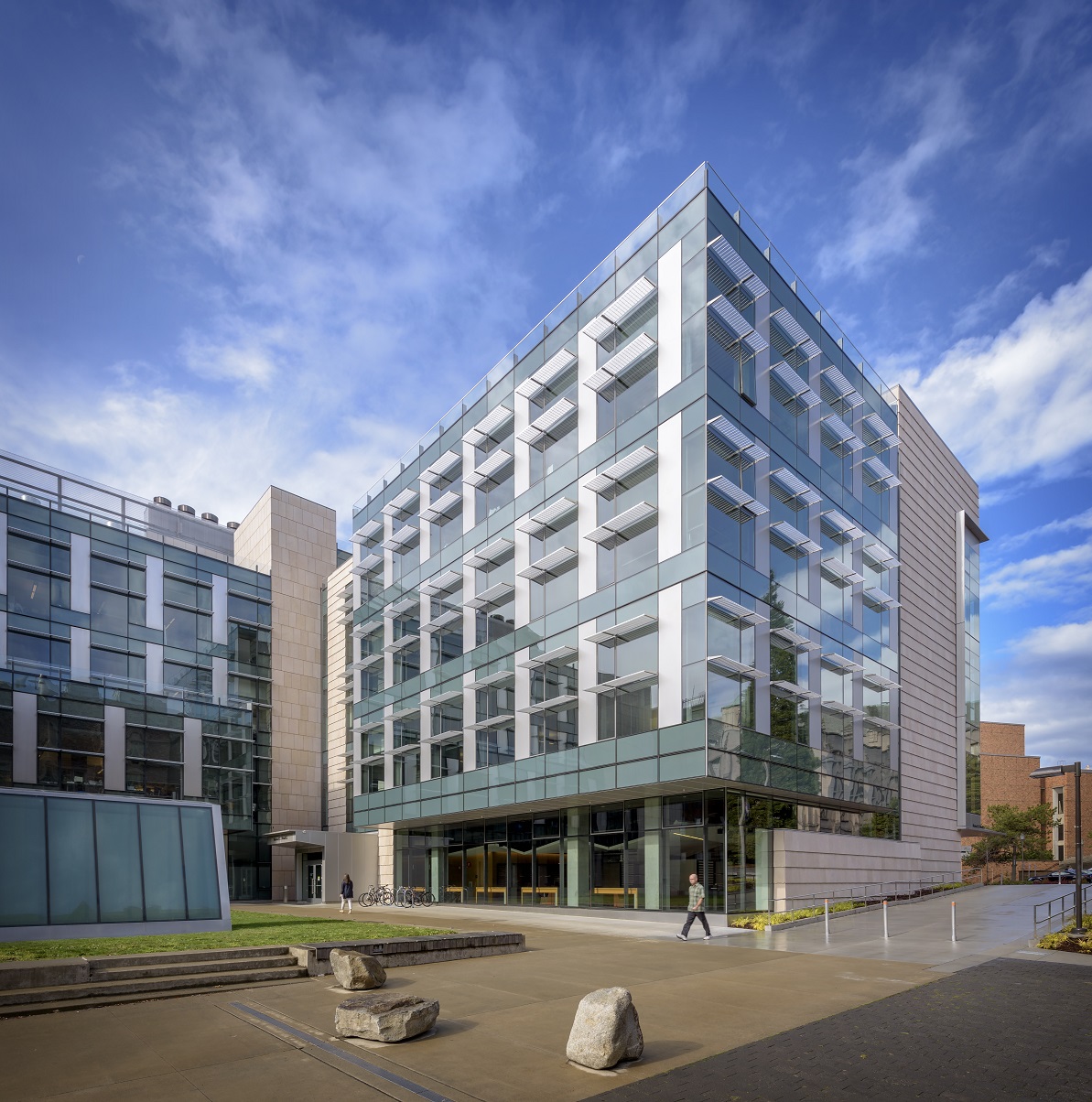
The NanoES Institute offers 35,000 square feet of labs (including wet and optical space), offices, meeting rooms, communal areas, and extremely low vibration/EMI areas in a brand-new building. This space creates an opportunity to scale up ongoing research efforts with strong momentum and to create new, high-impact programs or shared instrumentation facilities. To this end, NanoES is announcing a request for proposals. We are seeking inventive, well-thought-out ideas to leverage this space for maximum effect including, but not limited to, new center efforts and hiring initiatives endorsed by department chairs.