Skip to content

Prof. Edo Waks from the University of Maryland to give EE colloquium on 2/13/18

Interactions between light and matter lie at the heart of optical communication and information processing. Nanophotonic devices enhance light-matter interactions by confining photons to small mode volumes, enabling devices to operate at significantly lower energies.  In the strong coupling regime these interactions are sufficiently large to generate a nonlinear response with a single photon, an essential component for quantum information processing applications.  In this talk I will describe our effort to couple spin to light using nanophotonics. I will discuss an experimental demonstration of a quantum transistor, a fundamental building block for quantum computers and quantum networks, using a single electron spin that strongly interact with light through a nanophotonic cavity.  This device enables the spin to switch a single photon, and a single photon to flip the spin. I will discuss how the nanophotonic transistor can realize high fidelity all-optical spin readout, as well as a single photon transistor where one control photon can switch many signal photons. Finally, I will describe our recent effort to extend our results into the telecommunication wavelengths, and to integrate multiple devices on a chip to assemble integrated quantum photonic circuits.


Please join the Electrical Engineering Department for the 2017-18 Research Colloquium Series on Tuesday mornings, featuring experts who discuss current issues in the electrical engineering field. Talks are open to both students and the public.  Live streaming is available for most talks.
 

EE Colloquium – Silicon Integrated Circuit, Sensor, and System Approaches for Lab-on-CMOS Applications: November 28, 10:30 am, EEB 105

Title: Silicon Integrated Circuit, Sensor, and System Approaches for Lab-on-CMOS Applications

Date & Time: Tuesday, Nov. 28th, 10:30-11:30 am

Location: 105 EEB

Abstract: The Lab-on-CMOS research community leverages the power and economies of scale of modern silicon integrated circuits, built up over the previous fifty years for high-performance computation and imaging, for low-cost chemical and biological sensing applications. The integration of new materials, sensing modalities, and intelligent computation in CMOS-based sensor platforms enables a broad range of miniaturized diagnostic, therapeutic, and continuous monitoring systems. In this talk, I will present a survey of ongoing research in my lab focused on the chip-level development and system-level integration of IC-based sensors for physical, chemical, and biological sensing. This includes CMOS-integrated single-photon detectors, high dynamic range visible light sensing, on-chip high-voltage sensor biasing, low-voltage energy harvesting, and applications in radiation sensing and continuous biological monitoring. I will also describe our recently developed approach for the planar integration of IC-based sensors with microfluidic sample delivery using scalable, manufacturable processes.

Bio (IEEE): Matthew L. Johnston received the B.S. degree in electrical engineering from the California Institute of Technology, Pasadena, CA, in 2005, and the M.S. and Ph.D. degrees in electrical engineering from Columbia University, New York, NY, in 2006 and 2012, respectively.

He is currently an Assistant Professor in the School of Electrical Engineering and Computer Science at Oregon State University. He was co-founder and manager of research at Helixis, a Caltech-based spinout developing instrumentation for real-time PCR, from 2007 until its acquisition by Illumina in 2010. From 2012 to 2013 he was a postdoctoral scholar in the Bioelectronic Systems Lab at Columbia University. He is a co-founder of Chimera Instruments, which designs high-speed electrophysiology amplifiers for biophysics research, and previously founder of Bialanx, which was awarded an NSF SBIR Grant in 2013 for work in radiation biodosimetry.

Prof. Johnston currently runs the Sensors and Integrated Microelectronics Laboratory (SIM Lab) at Oregon State University, which leverages custom CMOS IC design and post-fabrication to build miniaturized sensor systems. His current research interests include integration of sensors and transducers with active CMOS substrates, lab-on-CMOS platforms for label-free chemical and biological sensing, and low-power distributed sensing applications.

Distinguished Practitioners in Nano-engineered Systems: December 5, 12:30 pm

Please join us for the inaugural lecture by Distinguished Practitioners in Nano-engineered Systems. This new seminar series is organized by the Institute for Nano-engineered Systems and focuses on individuals who are making outstanding contributions to the development of microsystems and nanotechnology with significant commercial and societal impact.

Speaker

Nena Golubovic, Ph.D.
Director, Physical Sciences
IP Group, Inc.

Tuesday, December 5, 12:30 – 1:20 pm
Anderson 223

Hard Science Innovation: Evolving Great Ideas into World-Changing Businesses

Our inaugural Distinguished Practitioner in Nano-engineered Systems will venture back in time and briefly cover the evolution of micro and nano electro mechanical systems (MEMS/NEMS), then focus the bulk of the presentation on early stage investing before finishing up with an outlook on collaborations between IP Group and UW.

Biography 

Nena joined IP Group in 2014, and currently oversees the Physical Sciences sector in North America.  As part of the senior management team she works on a variety of early stage investments transitioning from IP Group’s partner network research labs to the marketplace.

Nena has extensive experience developing and commercializing cutting edge micro-technology products for automotive, consumer and medtech industries.  She spent her 20-year career in medium public, private and small start-up environments.  Nena served as Vice President of Medical Products at Apogee Technologies where she led commercialization of micro-structured transdermal systems for drug delivery.  Prior to that she was Director of New Product Development at Standard MEMS where she led commercialization and manufacturing scaleup of the world’s first MEMS microphone. She collaborated with Xerox, Lexmark, Kavlico, Becton Dickinson and the likes in developing uniquely differentiated, micro-technology enabled, new product generations for applications across different market segments.  Nena was involved in various product development, go-to-market and management roles with several early stage start-up companies commercializing university technologies.

Nena holds a Ph.D. and M.S. in Electrical Engineering from the University of Cincinnati, and a B.S. in Engineering Physics from the University of Belgrade.

NanoES Building Ribbon Cutting Ceremony: December 4

 You’re Invited!

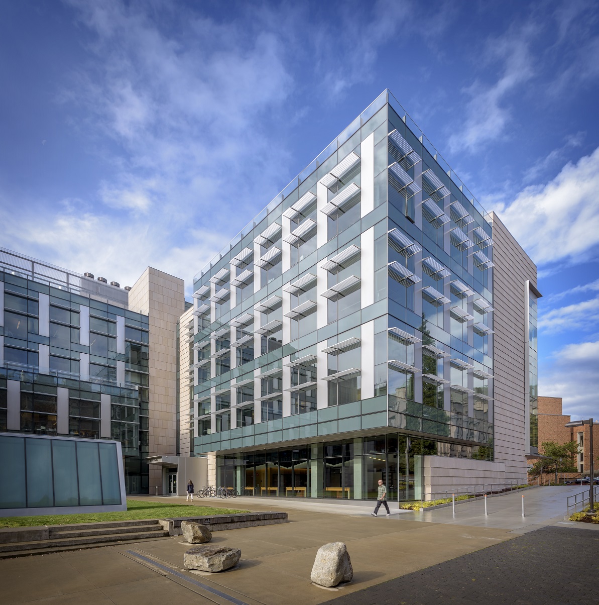
Participate in the kick-off of the Institute for Nano-engineered Systems as we celebrate the opening of the Nano Engineering & Sciences Building.

December 4, 2017// 4:00PM // NanoES Commons

We cordially invite you to the NanoES Building Ribbon Cutting Ceremony.

Join us afterwards for an evening of networking with food and drinks.

Please RSVP here.

Surface Characterization of Biomaterials Workshop: July 31-August 2

July 31 thru August 2, 2017
University of Washington, Seattle WA
Workshop flyer

This 2.5 day workshop includes lectures and surface analysis demonstrations. Demonstrations on NESAC/BIO instruments will provide application examples for the material covered in the workshop lectures. Attendees will learn the capabilities of biomedical surface analysis methods and how to intelligently review data received from surface analysis laboratories. NESAC/BIO faculty and staff will address the following topics at this workshop:

  • Introduction to Surface Analysis  (David Castner)
  • Electron Spectroscopy for Chemical Analysis  (Lara Gamble)
  • Secondary Ion Mass Spectrometry  (David Castner)
  • Sum Frequency Generation  (Patrik Johansson)
  • Contact Angle Measurements  (Allan Hoffman)
  • Surface Modification (Allan Hoffman)
  • Multivariate Data Analysis  (Dan Graham)
  • Scanning Probe Microscopy  (Micah Glaz)
  • Surface Plasmon Resonance  (David Castner)
  • Quartz Crystal Microbalance (David Castner)
  • Near Edge X-ray Absorption Fine Structure  (Lara Gamble)
  • Multi-technique Biomedical Surface Analysis  (Buddy Ratner)
  • Instrument Demonstrations

To register and obtain further information please visit the NESAC/BIO Workshop website: http://www.nb.uw.edu/content/nesacbio-workshop


For more information, please contact
Prof. David G. Castner
Director, National ESCA & Surface Analysis Center for Biomedical Problems, an NIH-funded resource
Director, Molecular Analysis Facility
Molecular Engineering & Sciences Institute
Departments of Bioengineering & Chemical Engineering
Box 351653
University of Washington
Seattle, WA  98195-1653  USA
phone:  206-543-8094
fax:  206-221-7451
e-mail:  castner@uw.edu
web:  www.nb.uw.edu