April 7, 2026
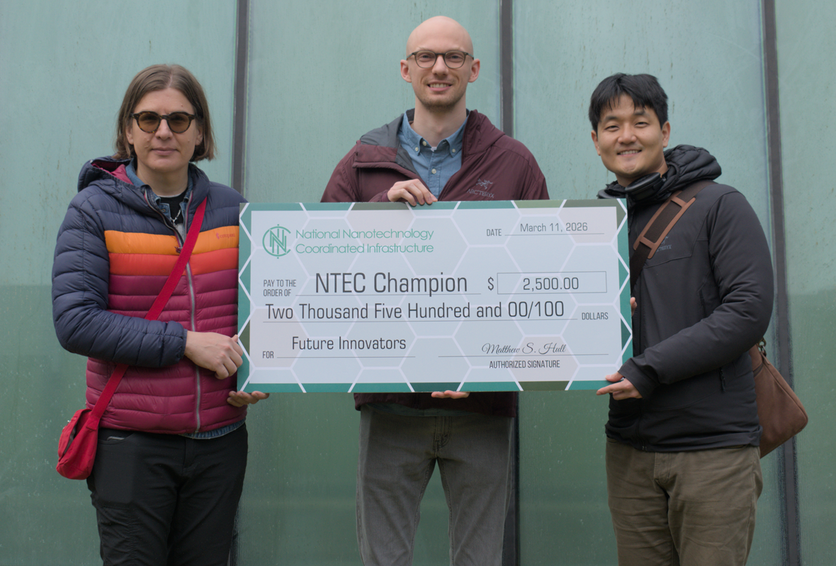
A team from University of Washington Chemical Engineering Professor Lilo Pozzo’s research group took first place in the National Nanotechnology Coordinated Infrastructure (NNCI) NanoTechnology Entrepreneurship Challenge (NTEC), held during the Future Innovations session on March 11 at TechConnect in Raleigh, North Carolina.
NTEC provides experiential entrepreneurship education for teams led by undergraduates, graduate students and post-doctoral scholars. NTEC teams learn about the importance of customer discovery and how to leverage NNCI resources to develop a nanotechnology-enabled minimum viable product (MVP). The seven-week, virtual “at-your-pace” program culminates in a “pitch” event where teams share their progress with business leaders.
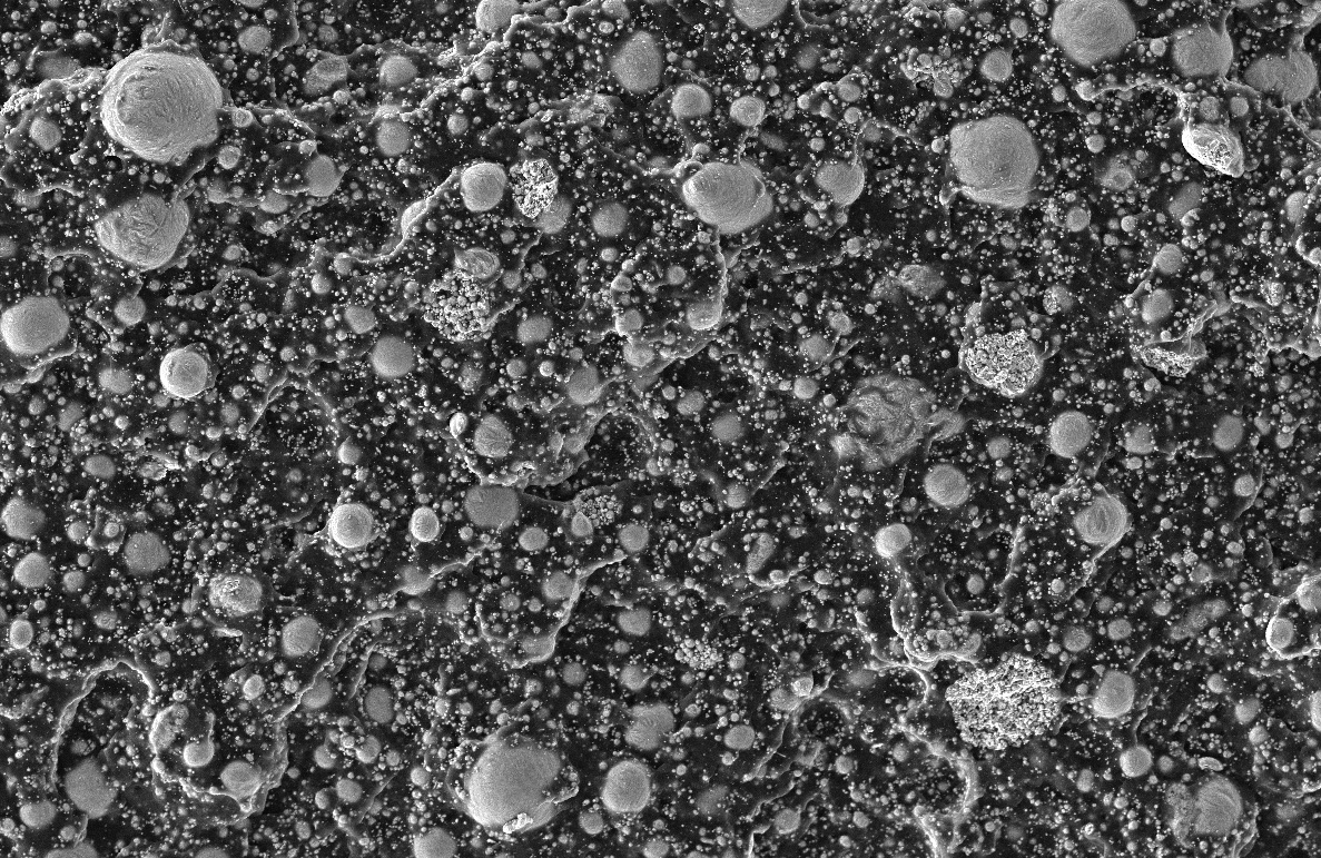
Led by CoMotion Postdoctoral Entrepreneurship Fellow Kevin Lee and PhD student Zach Wylie, the winning project from the Pozzo Research Group involves the development of next generation high-power-density battery electrodes for power-hungry applications that traditionally relied on diesel. The group will use the $2,500 award from NNCI to continue development and validation of their technology based on the group’s proprietary nanoparticles.
“Through customer-discovery work conducted with NNCI’s NTEC program, we’ve gained a clear understanding of the pain points faced by legacy battery manufacturers,” said Lee and Wylie.
Looking ahead, Lee and Wylie “plan on using NNCI’s facilities such as the Molecular Analysis Facility (MAF) and Washington Nanofabrication Facility (WNF) to characterize our material under industry-relevant conditions and generate data that manufacturers require to evaluate and ultimately adopt our material.”