Skip to content

New metasurface design can control optical fields in three dimensions

A team led by NanoES faculty member Arka Majumdar, an assistant professor of electrical and computer engineering and physics, has designed and tested a 3D-printed metamaterial that can manipulate light with nanoscale precision. As they report in a paper published October 4 in the journal Science Advances, their designed optical element focuses light to discrete points in a 3D helical pattern. Designing optical fields in three dimensions could enable creation of ultra-compact depth sensors for self-driving cars, as well as improved components for virtual- or augmented-reality headsets.

Defects Wanted; Apply Here – Q&A with physicist Kai-Mei Fu

NanoES faculty member and professor of electrical engineering and physics recently sat down with APS Physics. Kai-Mei studies the properties of atomic defects in materials with the goal of using these normally unwanted flaws to create quantum technologies for secure communication. She is also the co-chair of QuantumX, a University of Washington initiative seeking to facilitate and support activities that will accelerate quantum discoveries and technologies

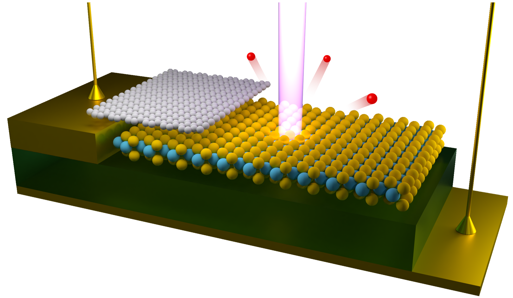
First-ever visualizations of electrical gating effects on electronic structure could lead to longer-lasting devices

UW physicists David Cobden and Xiaodong Xu, in collaboration with colleagues at the University of Warwick, developed a technique to measure the energy and momentum of electrons in operating microelectronic devices made of atomically thin — so-called 2D — materials. Their findings, published last week in the journal Nature could lead to new, finely tuned, high-performance electronic devices.