
This post is part of a series of profiles highlighting faculty research in the Institute of Nano-engineered Systems
Peter Pauzauskie, associate professor of materials science and engineering, joined the Institute for Nano-Engineered Systems (NanoES) in spring 2018. Pauzauskie’s research group synthesizes atomically-precise nanoscale materials to understand and harness their optical and electronic properties for potential applications in next-generation quantum sensors, advanced biomedical devices, and solid-state laser refrigeration.
“We are specifically interested in defects and impurities within nanocrystals, and how we can make these defects useful,” says Pauzauskie. “We can control the location and chemical identity of defects within the crystal’s lattice down to the atom, which is also known as doping, or point-defect engineering. Ultimately, we are trying to develop a rational understanding of crystal growth based on our manipulation of temperatures and pressures during the synthesis process.”
“Peter’s research on nanocrystal synthesis and optoelectronics align directly with our research focuses, like integrated photonics,” says Karl Böhringer, NanoES director and electrical and computer engineering professor. “As an institute, we are trying to facilitate new collaborations between faculty in the College of Engineering and across the University of Washington in order to bring about truly innovative research. Peter’s expertise and collaborative spirit will be invaluable to a wide range of possible research efforts.”
Laser refrigeration with nanocrystals
Pauzauskie’s research group engineers nanocrystals with unique properties. Typically, matter warms when illuminated with a laser because light energy is translated into molecular vibrations that produce heat. Pauzauskie’s team developed a special type of ceramic nanocrystal that, when illuminated with an infrared laser, emits light with slightly more energy than it absorbed. This loss of energy across the whole crystal results in a decrease in the crystal’s temperature, and subsequent cooling of its surroundings. When Pauzauskie’s team suspended one of these crystals in water, they showed they could “laser-cool” the water by 36ºF, nearly to water’s freezing point.
“Our group was the first to refrigerate water using laser cooling of nanocrystals,” says Pauzauskie. “We are especially excited about potential biological applications at the cellular level.” For example, laser cooling with nanocrystals could be used to precisely cool portions of a cell in order to slow down rapidly occuring processes, allowing scientists to observe what is going on without damaging or killing the cell.
Nanodiamonds for next-generation computing and biotechnology

Due to their rigid crystal lattices, diamonds are the hardest and most thermally conductive bulk material. Though they are efficient conductors of heat, most diamonds do not conduct electrons efficiently. However, as is the case for many materials, different properties emerge at the nanoscale — especially when impurities are introduced. Thus, by manipulating a nanodiamond’s composition, researchers can modify its optical and electronic properties. The nanodiamonds synthesized in the Pauzauskie lab are created by submitting doped carbon aerogels, which are styrofoam-like solids made of nanoparticles, to extremely high pressures within a laser-heated diamond anvil cell. Through funding from the National Science Foundation, Pauzauskie’s team is optimizing the conditions necessary to create nanodiamond materials that are capable of conducting electrons for future optical and electronic devices.
Nanodiamond materials also show great promise in a variety of other applications. For instance, point defects in nanodiamonds could form the foundation for future quantum computers, while nanodiamonds functionalized with biological molecules could be used to advance magnetic resonance imaging or drug delivery for cancer treatment.
Contactless optical thermometers
Photoluminescent materials can absorb light at many different energy levels, but re-emit light at specific wavelengths. The emission wavelength largely depends on the material’s makeup and theenergy of the incoming light, but can also vary based on the temperature of the material itself. Pauzauskie’s group harnessed this temperature dependence to create “optical thermometers” comprised of crystals doped to an atomically-precise level with the elements ytterbium and erbium, which luminesce different shades of green light.
With knowledge of the crystal’s precise makeup and the ability to control the incoming light with a laser, Pauzauskie’s team can calculate the precise wavelengths that the crystal will emit at a particular temperature. At higher temperatures, the green luminescence will be bluer in color, whereas at lower temperatures, the luminescence will be redder in color. Thus, by simply shining a laser at one of these crystals, researchers can indirectly determine the temperature of the crystal’s surroundings. The potential applications for this contactless optical thermometer span from cell culture to instrumentation for airplanes and smart buildings.
Cross-cutting collaborations
Pauzauskie holds a dual appointment at the Pacific Northwest National Laboratory (PNNL), where he is a staff scientist and a co-investigator on materials research with Dr. Jim De Yoreo, chief scientist for materials synthesis and simulation across scales at PNNL. De Yoreo is also an affiliate professor at UW and co-director of the Northwest Institute for Materials Physics, Chemistry, and Technology (NW IMPACT), a joint research collaboration between PNNL and UW. Both De Yoreo and Pauzauskie occupy space on the 2nd floor of the NanoES building. With respect to the partnership with PNNL, Pauzauskie says, “It is a major advantage because we rely on their advanced characterization facilities to observe, quantify, and understand the atomically precise materials that we’re making at UW.”
At PNNL, Pauzauskie’s team uses a materials characterization technique known as atom probe tomography (APT) to pick apart a crystal atom-by-atom and create a 3-dimensional map of the crystal’s lattice structure. “This technique is similar to mapping out the location of all of the stars in a galaxy one-by-one, except we are studying individual atoms or ions within a crystal on Earth,” Pauzauskie explains. This incredible level of detail is useful when characterizing point-defect crystals, as the concentration of dopants can be as low as parts-per-million.
“Some of the most interesting phenomena in nanoscience can be found at the intersections of different fields,” says Pauzauskie. “It’s only natural that new collaborations happen when groups coexist in a dynamic space like NanoES — you never know when graduate students, post-docs, and their faculty advisers will be inspired over a cup of coffee.”
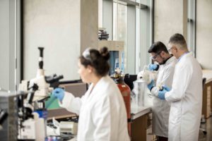
The Pauzauskie Research Group maintains office space, a wet lab for nanocrystal synthesis, and a lab for laser spectroscopy experiments in the NanoES building.