April 29, 2025
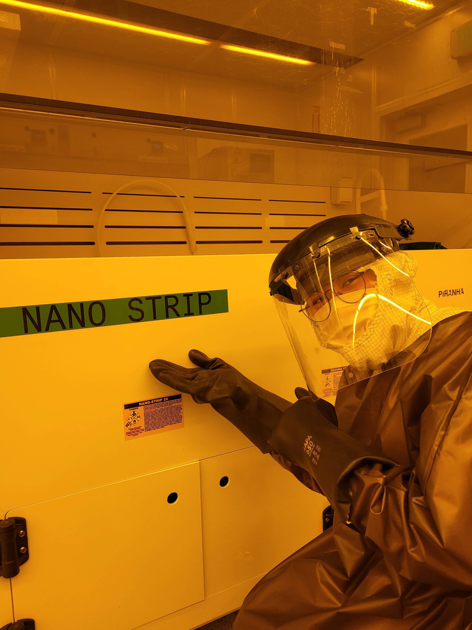
Four years ago, as an Engineering Dean’s Scholar, Jimmy Phan was listening to a lecture from the College of Engineering’s associate dean, Dan Ratner. Ratner told Phan’s cohort about the Washington Nanofabrication Facility (WNF), an open-access nanofabrication facility at the UW, and the opportunities for undergraduates to work there. By his second year of school, Phan was employed as an undergraduate lab assistant in the facility. Students working in the WNF have a unique opportunity to receive on-the-job training from research engineers and network with professionals in advanced electronics, nanotechnology, semiconductors and fabrication-related jobs. Thanks to his work at the WNF, Phan interned at Intel last summer and will work there full-time after graduating with a mechanical engineering degree this spring.
WNF: How does your work at the WNF complement your education in mechanical engineering?
Phan: For me, the two don’t really overlap, so I had a lot to learn in the WNF. Before working there, I didn’t know much about the semiconductor industry – I thought I’d work in aerospace, robotics or manufacturing. But I learned so much at the WNF, and the connections I made there helped me get my internship at Intel.
WNF: What was the internship at Intel like, and how did your work in the WNF help?
Phan: My interview with Intel lasted 30 minutes, of which 20 were spent explaining the work in their semiconductor fabrication plant, so I knew what they were talking about. The work there is like ours but at a much larger scale. I worked on metal deposition (layering metal onto the semiconductor wafers) and wafer grinding together with other interns. They didn’t have the same experience I had—most had never been in a clean room and had a lot to learn about the processes. There is a lot more automation and more technicians in the industry, but I enjoyed the work and put a lot of the theory I learned in school and the skills I gained at the WNF to work.
Once I graduate, I’ll be with the same team I worked with last summer. I worked at the Oregon campus, and the work helped me realize my interests. I don’t think many people know about all the job opportunities in the semiconductor industry or even know of a clear path to becoming a cleanroom technician. I can say I would have neither without the WNF.
WNF: What did you learn from the WNF that you will use at Intel?
Phan: I learned from equipment engineering lead Steven Spalsbury, facilities lead Sarice Jones, and photolithography lead Jean Nielsen. I gained troubleshooting skills and learned how to fix tools. I also learned about the facilities side of running the WNF and even developed my own process for using the chemicals for one of their tools.
Staff at the WNF have been providing training to students interested in working in the industry through short courses and undergraduate jobs and I’ve been able to help with some of that work too.