The Northwest Nanotechnology Infrastructure, of which the Institute for Nano-engineered Systems leads, is one of NNCI’s 16 member sites. Researchers are invited to submit images of their work taken at NNCI facilities (which at the UW includes the Washington Nanofabrication Facility and the Molecular Analysis Facility) for consideration for the categories of Most Stunning, Most Whimsical and Most Unique Capability.
The winners will be entered into a network-wide competition. Public voting begins October 5.
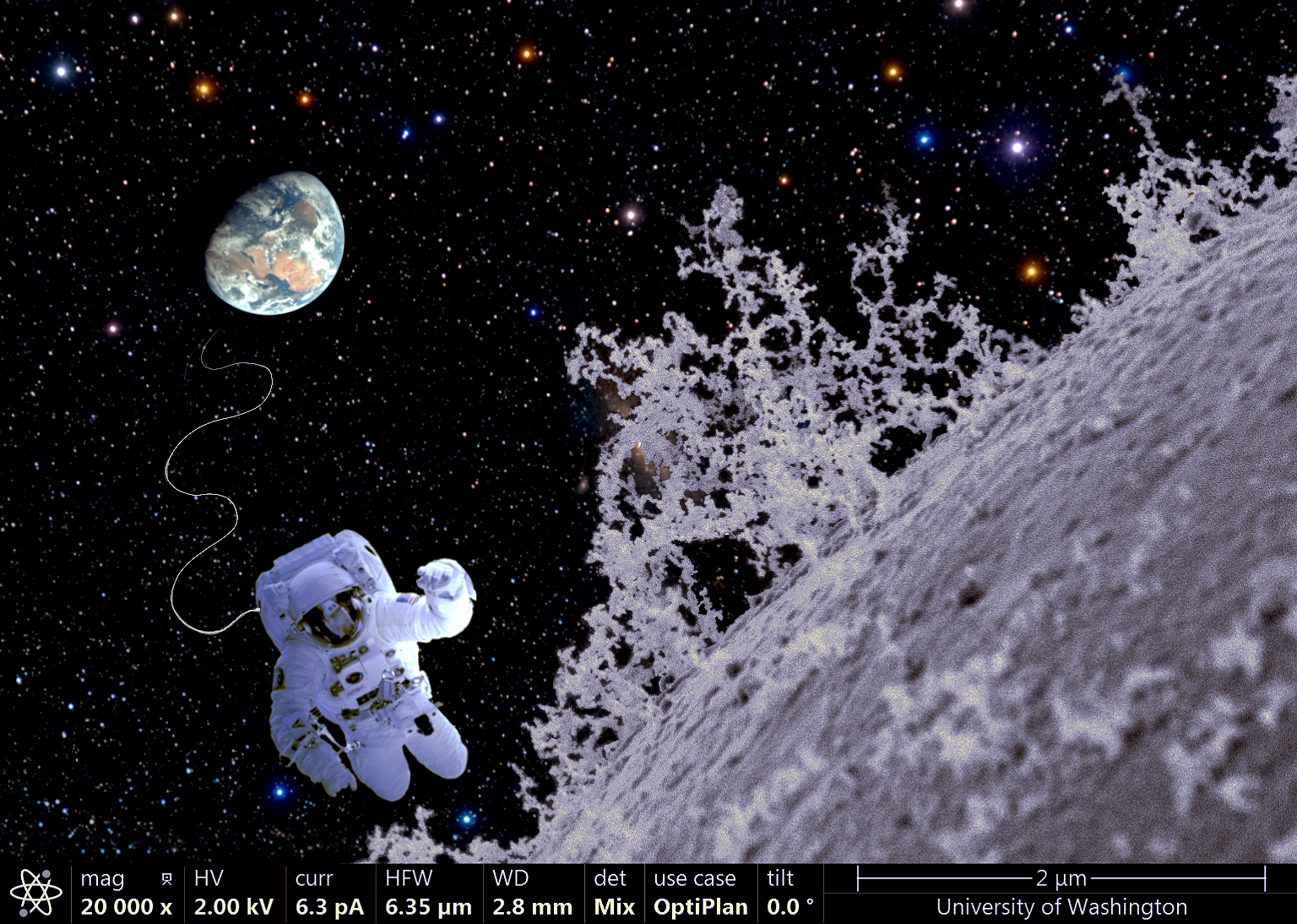
Most Whimsical – Winner
Space Debris Sarah Waddell, Materials Science and Engineering Graduate Student in the Arola Lab
Taken on an Apreo SEM in the Molecular Analysis Facility
Titanium nanoparticles can be seen in networks upon spherical powder ejected during titanium 3D-printing. These nanoparticles are a byproduct of the laser-based printing process formed by the solidification of vaporized metal, creating an appearance similar to an alien planet.
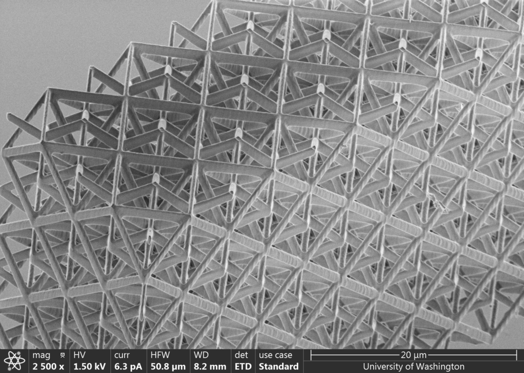
Most Stunning – Winner
Micro-Trusses Zainab Patel, Materials Science & Engineering Graduate Student in the Meza Lab
Taken on an Apreo SEM in the Molecular Analysis Facility
Damage resist truss made of two interpenetrating lattices made using two-photon lithography aka nanoscale 3D printing.
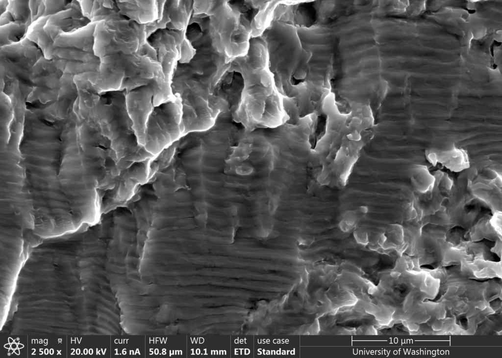
Most Unique Capability – Winner
Plenty of Waves at the Bottom Mohammad Sayem Bin Abdullah, Mechanical Engineering Graduate Student in the Mamidala Lab
Taken on an Apreo SEM in the Molecular Analysis Facility
Large waves are hitting scattered mountainous islands during a tsunami. The waves are the gradual progression of a crack in additively manufactured (AM) Titanium. The tsunami is resembling the high-stress amplitude used during the fatigue experiment of the specimen. The crack grows at ~1 μm/cycle. This image confirms the ductile behavior in cyclic loading (fatigue), a prerequisite for large-scale manufacturing of titanium through AM processes. The specimen was built at 30 degrees using the Electron Beam Melting process, a novel AM technique to 3D print high-temperature metals. The geometric variability is being investigated to study the sustainability of the process.
2022 Featured Submissions
Order within disorder by Ankush Nandi, Graduate Student
Entropy-stabilized oxides can trap upto 5 cations in a crystal structure (something entropy shouldn’t allow!), but this order is achieved using combustion synthesis initiated by electromagnetic fields to fabricate these ceramics in less than 20 seconds outside a furnace. This is a SEM image of (Mg0.2Co0.2Ni0.2Cu0.2Zn0.2)O ESOs with graphene as susceptor for combustion synthesis.
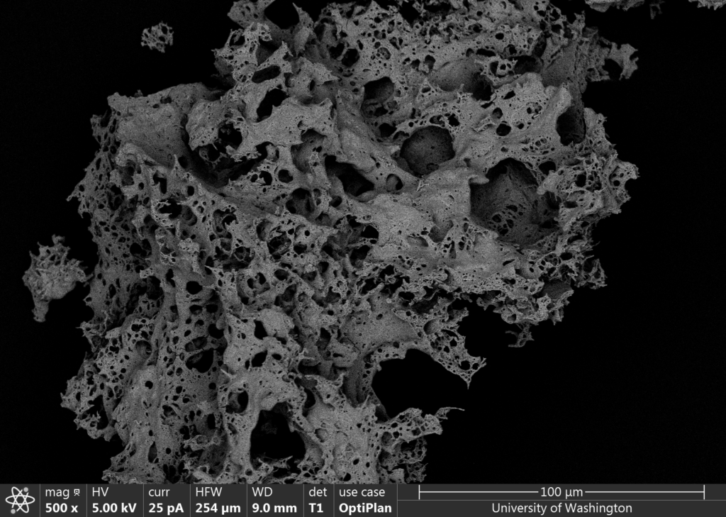
The extreme survival by Nishita Anandan, Postdoctoral Fellow
The architected nano-ceramic shell structure survived laser induced shock while the Titanium film around it spalled. A proof that materials can be architected at the nanoscale to withstand significant shock!
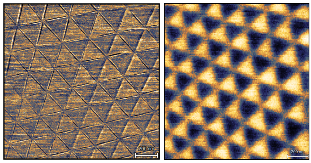
Polarized Domains in a Twisted hBN Moire by Jordan Fonseca, Graduate Student
When monolayers of hexagonal boron nitride are stacked with a small twist angle, alternating stacking domains emerge that support an out-of-plane electric polarization. The domain walls and polarized domains can be imaged with piezoresponse force microscopy (left) and kelvin probe force microscopy (right), respectively.
Of peas and pods by Emily Miura-Stempel, Graduate Student
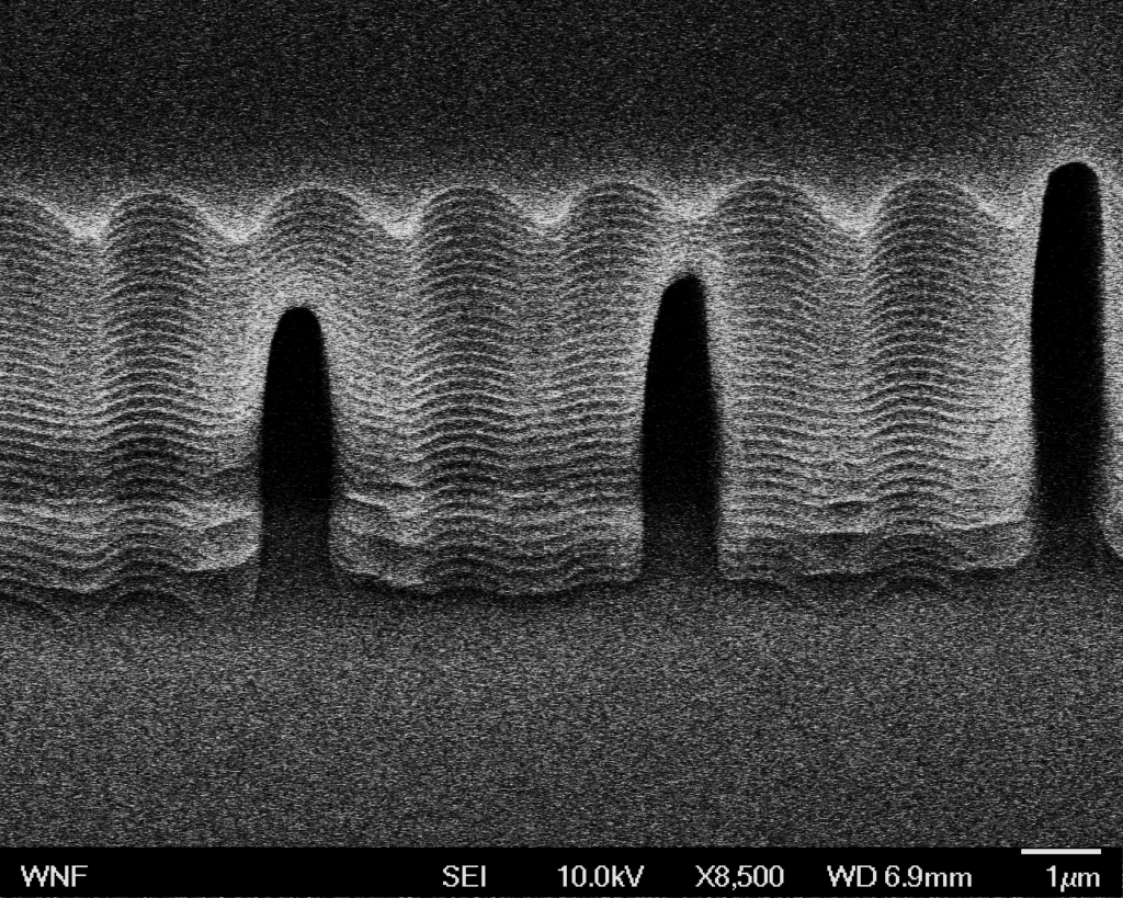
Caves at the Cliffs by Brant Hempel, Staff Scientist
This is an image of tunnels created in a photoresist layer on the silicon wafer using a 2-photon 3D printer. The image also showed standing waves created by the interference pattern of light as it is reflected off the substrate.
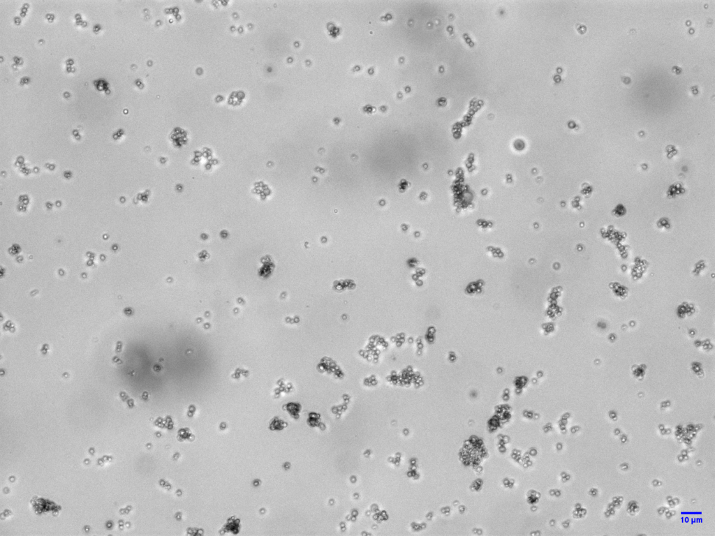
ArtiFusially Together by Widianti Sugianto, Graduate Student
A brightfield image of self-assembled phospholipid vesicles (micron-sized) containing transcription/translation systems for creating ‘synthetic’ cells. While unalive, some ‘synthetic’ cells started to move and aggregate/fuse themselves.
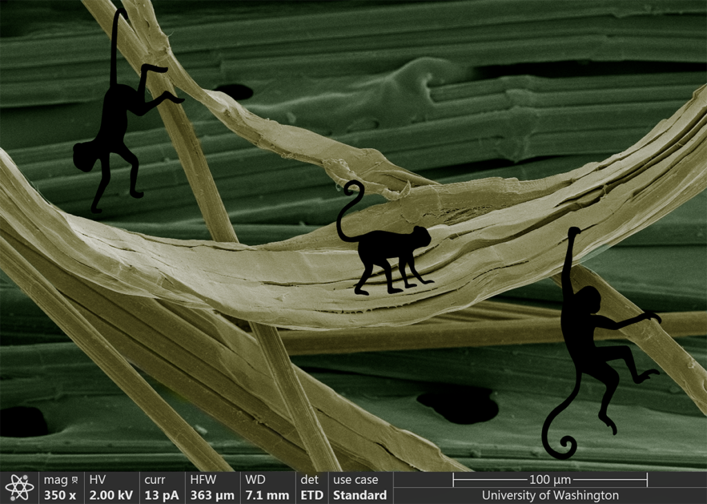
MicroMonkeys by Colin Marquis, Graduate Student
High strength polymer fibers show surface smoothing and shape change after passing through a 3D printing nozzle at temperatures near their melting point. These fibers show great potential for combination with other plastics to create exceptionally strong 3D printing filaments. Peering through the eye of a scanning electron microscope a jungle of fibers is revealed, well suited for playful MicroMonkeys to explore.
Balance of Yin Yang (Nature and Technology) by Gokce Altin Yavuzarslan, Graduate Student
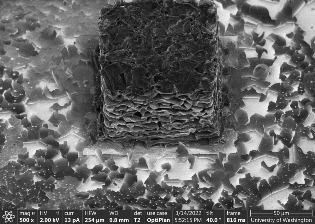
While humankind has made tremendous progress in technology during the last few centuries, unfortunately, it has done a lot of damage to nature. Environmental pollution is one of these harms. We designed 3D printable engineered living materials (ELMs) to overcome non-degradable waste accumulation in nature. ELMs are biodegradable smart materials that contain microorganisms in a polymer matrix. This SEM image shows the cross-section of 3D printed ELM in which genetically modified S. cerevisiae cells are embedded in a protein-based polymer. Yin and Yang traces in the image are a reference to the balance between nature and the ELM we have developed.
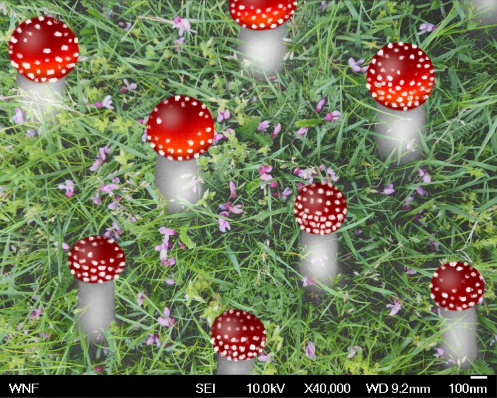
Dielectric Nano Fly Agaric by Zheyi Han, Graduate Student
The silicon nitride nano-posts are etched with circular alumina pattern masks to construct an ultra-thin meta-optic lens for the visible spectrum. The specific combination of processing gases and chamber pressure conditions creates the undercut beneath the hard mask. When inspected under the scanning electron microscope, the nano-posts with caps appear like a group of young fly agaric mushrooms in the magical woodland at the bottom.