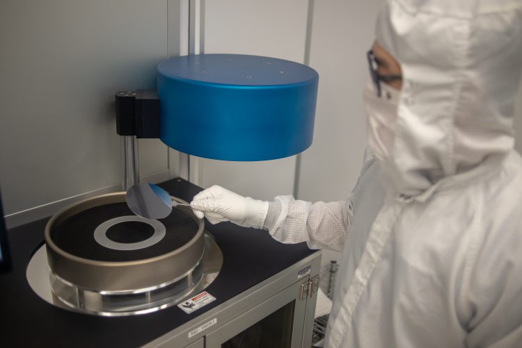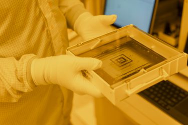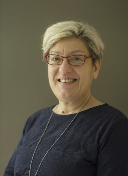
Seattle, WA – Dr. Maria Huffman is the new director of the University of Washington’s Washington Nanofabrication Facility (WNF), the largest publicly accessible nanofabrication facility in the Pacific Northwest with 15,000 square feet of combined clean room, laboratory, and user spaces. WNF provides researchers and engineers with the resources and expertise necessary to fabricate materials, structures, and devices at the nanoscale for applications ranging from aerospace and information technology to medical research
“I am deeply honored to support the work of people pushing the boundaries of nanoscience and engineering to advance new technologies and devices at one of the world’s preeminent public universities and research institutions,” said Huffman. “WNF has an exceptional staff of engineers who are both immensely professional and knowledgeable about nanofabrication processes and tools. I am looking forward to working with them as well as collaborating with partners from across the university to offer the best services possible for users of our facility.”
Huffman joins WNF from Lund University in southern Sweden, where she was the director of the Lund Nano Lab (LNL), an open-access nanofabrication facility serving researchers at the university, in the region, and beyond. LNL is part of a network of university clean rooms in Sweden (Myfab) as well as the broader nanofabrication and characterization infrastructure in Europe.
Previously, Huffman spent over 30 years working in the semiconductor and solar industries in a variety of research and development as well as manufacturing roles. She managed small teams to whole departments developing next-generation technology solutions for thin-film solar, semiconductor processing, and laser optics production. Throughout her career, Huffman has interfaced with customers and clients as a technical liaison and consultant, working with technical teams to engineer new and improved manufacturing processes.

WNF is part of the UW College of Engineering’s Institute for Nano-engineered Systems (NanoES), which seeks to catalyze innovative, interdisciplinary, and industry relevant research in the design, fabrication, and integration of scalable nano-engineered devices and systems. NanoES oversees the Northwest Nanotechnology Infrastructure, which is one of 16 National Nanotechnology Coordinated Infrastructure (NNCI) sites funded by the National Science Foundation (NSF). Both WNF and the UW Molecular Analysis Facility (MAF) are part of the NNCI network of open-access nanotechnology user facilities.
“Maria’s wealth of experience in both academia and industry will serve WNF as it continues to evolve and offer new capabilities,” said Karl Böhringer, NanoES director and professor of electrical and computer engineering and bioengineering. “Over the past seven years, WNF has grown substantially, with more academic and industrial users leveraging WNF tools and processes to innovate in an efficient and cost-effective manner. I look forward to seeing this world-class facility thrive under Maria’s leadership.”

In 2011, UW assumed ownership of the nanofabrication facility previously run by the Washington Department of Commerce. UW invested $37 million in 2015 to renovate WNF – tripling the size of the facility and upgrading the clean room infrastructure – enabling the facility to accommodate more equipment and users and giving users access to a more reliable ISO Class 5/6 clean room in which to make high quality devices.
Said Huffman, “UW is a pioneer in many areas, from quantum information science to population health. WNF’s robust infrastructure can help accelerate innovation in areas the university is committed to pursuing. My goal for WNF is to tap into new applications of nanofabrication, inside and outside the university, bringing in new users from different disciplines who are doing groundbreaking work.”
